| CPC G02B 6/4201 (2013.01) [G02B 6/34 (2013.01); H01L 25/0756 (2013.01); H01L 33/62 (2013.01); G02B 6/12019 (2013.01); G02B 6/30 (2013.01); H01L 23/367 (2013.01); H01L 33/58 (2013.01); H04B 10/40 (2013.01)] | 22 Claims |
|
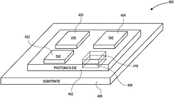
1. A photonics die comprising:
a first side of the photonics die and a second side of the photonics die opposite the first side of the photonics die;
an optical interconnect at the second side of the photonics die to transmit light signals to or to receive light signals from outside the photonics die;
a photonics integrated circuit (PIC) optically coupled with the optical interconnect;
one or more electrical connectors on the first side of the photonics die, wherein the one or more electrical connectors are electrically coupled with the PIC; and
electrical circuitry to electrically couple a first location on the first side of the photonics die with a second location on the first side of the photonics die, wherein a first chip is to be disposed and electrically coupled with the first location on the first side of the photonics die, and wherein a second chip is to be disposed and electrically coupled with the second location on the first side of the photonics die.
|