US 12,135,457 B2
Liquid crystal optical element and method for manufacturing the same
Koichi Igeta, Tokyo (JP); Shinichiro Oka, Tokyo (JP); Yasushi Tomioka, Tokyo (JP); Junji Kobashi, Tokyo (JP); and Hiroyuki Yoshida, Suita (JP)
Assigned to Japan Display Inc., Tokyo (JP); and OSAKA UNIVERSITY, Suita (JP)
Filed by Japan Display Inc., Tokyo (JP); and OSAKA UNIVERSITY, Suita (JP)
Filed on Feb. 2, 2024, as Appl. No. 18/430,928.
Application 18/430,928 is a continuation of application No. PCT/JP2022/021569, filed on May 26, 2022.
Claims priority of application No. 2021-128317 (JP), filed on Aug. 4, 2021.
Prior Publication US 2024/0176074 A1, May 30, 2024
Int. Cl. G02B 6/27 (2006.01); G02F 1/13 (2006.01)
CPC G02B 6/2726 (2013.01) 12 Claims
OG exemplary drawing
 
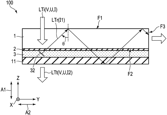
1. A liquid crystal optical element comprising:
an optical waveguide comprising a first main surface and a second main surface opposed to the first main surface;
an alignment film disposed on the second main surface;
a liquid crystal layer which overlaps the alignment film, which comprises cholesteric liquid crystals, and which reflects at least part of light incident through the optical waveguide toward the optical waveguide; and
a transparent first protective layer which overlaps the liquid crystal layer, and which is formed of a water-soluble polymer or a fluorine-based resin.