| CPC G02B 6/1225 (2013.01) [G02B 6/12019 (2013.01); G02B 2006/1213 (2013.01); G02B 2006/12173 (2013.01); G02B 2006/12176 (2013.01)] | 20 Claims |

|
1. A method, comprising:
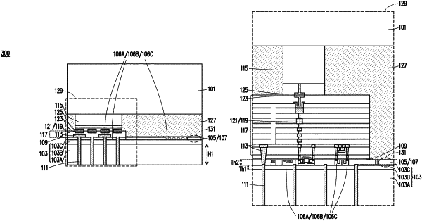
providing a first layer between a second layer and a semiconductor substrate, the first layer being between the semiconductor substrate and the second layer, the first layer having a first surface facing the semiconductor substrate and a second surface facing the second layer;
forming a first waveguide in the second layer;
forming a photonic die over the first waveguide;
after providing the first layer, the second layer and the semiconductor substrate, forming a first cavity in the semiconductor substrate and exposing a portion of the first surface of the first layer to form an exposed first surface of the first surface of the first layer;
filling the first cavity with a first backfill material on the exposed first surface of the first layer; and
electrically coupling an electronic die to the photonic die.
|