| CPC H01L 21/4857 (2013.01) [H01L 21/4828 (2013.01); H01L 21/4871 (2013.01); H01L 21/76871 (2013.01); H01L 23/49894 (2013.01); H05K 3/181 (2013.01); H05K 3/3452 (2013.01)] | 10 Claims |
|
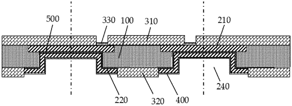
1. A manufacturing method for a package substrate, comprising:
providing a bearing plate, manufacturing a pattern of a first circuit layer on the bearing plate, and depositing metal to form the first circuit layer;
manufacturing a pattern of a cavity on an upper surface of the first circuit layer, depositing and etching metal to form a metal cavity, laminating a dielectric layer on a surface of the metal cavity, and performing thinning to expose an upper surface of the metal cavity;
forming a second circuit layer by removing the bearing plate, etching the metal cavity to expose the cavity, depositing metal on a surface and side walls of the cavity and a surface of the dielectric layer, and performing pattern manufacturing and etching;
forming a first solder mask layer and a second solder mask layer correspondingly on surfaces of the first circuit layer and the second circuit layer, and performing pattern manufacturing on the first solder mask layer or the second solder mask layer to form a bonding pad; and
cutting the cavity, the first circuit layer, the second circuit layer, the first solder mask layer and the second solder mask layer.
|