| CPC H01L 21/3086 (2013.01) [H01L 21/3081 (2013.01)] | 20 Claims |

|
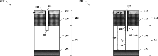
1. A method for forming a semiconductor device, comprising:
forming a first metal layer on top of an amorphous mask layer disposed over a substrate;
patterning the first metal layer and the amorphous mask layer using a metal etch hard mask layer to form an opening in the amorphous mask layer;
forming a second metal layer that extends along vertical sidewalls of the opening;
forming a first recess partially extending into the substrate using the first metal layer and the second metal layer as a first etch mask;
forming a third metal layer that extends along vertical sidewalls of the first recess; and
forming a second recess below the first recess using the first to third metal layers as a second etch mask.
|
|
12. A method for forming a semiconductor device, comprising:
forming a mask layer over a substrate;
forming a first metal layer comprising a first metal over the mask layer;
forming an opening in the first metal layer and the mask layer using a patterned metal etch hard mask layer;
forming a first portion of a metal spacer comprising a second metal along sidewalls of the opening;
etching the substrate to form a first recess using the first metal layer and the first portion of the metal spacer as a first etch mask;
forming a second portion of the metal spacer comprising a third metal along sidewalls of the first recess; and
etching the substrate to form a second recess below the first recess using the first metal layer and both of the first and second portions of the metal spacer as a second etch mask.
|
|
19. An apparatus, comprising:
a first chamber configured to house a substrate overlaid by a mask layer and perform deposition of a first metal layer over the mask layer;
a second chamber configured to form an opening through the first metal layer and the mask layer using a patterned metal etch hard mask layer;
a third chamber configured to perform deposition of a second metal layer to extend along vertical sidewalls of the opening;
a fourth chamber configured to etch a horizontal portion of the second metal layer;
a fifth chamber configured to form, based at least on a remaining vertical portion of the second metal layer, a first recess extending into the substrate;
a sixth chamber configured to perform deposition of a third metal layer to extend along vertical sidewalls of the first recess;
a seventh chamber configured to etch a horizontal portion of the third metal layer; and
an eighth chamber configured to form, based at least on a remaining vertical portion of the third metal layer, a second recess further extending into the substrate.
|