| CPC G11C 11/4091 (2013.01) [G11C 11/4094 (2013.01); G11C 11/4096 (2013.01)] | 18 Claims |

|
1. A method of operating a memory device, comprising:
precharging a pair of true and complementary bit lines to an equivalent voltage concurrently with precharging a pair of true and complementary sense bit lines within a sense amplifier to the equivalent voltage; then
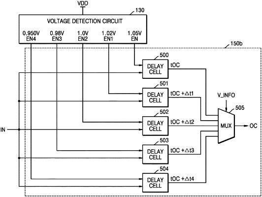
transferring charge associated with offset noise from the true bit line to the complementary sense bit line concurrently with transferring charge associated with the offset noise from the complementary bit line to the true sense bit line, so that a voltage difference is established between the true sense bit line and the complementary sense bit line, wherein the memory device is configured such that a duration of said transferring charge associated with the offset noise is adjusted in response to changes in magnitude of an internal power supply voltage within the memory device; then
reading a logic state of a memory cell within the memory device by transferring charge between the memory cell and the true bit line, concurrently with equilibrating voltages on the true and complementary sense bit lines; and then
sensing and amplifying a voltage difference between the true and complementary sense bit lines in response to activating an amplifier circuit within the sense amplifier, said amplifier circuit electrically connected to the true and complementary sense bit lines and responsive to voltage signals developed on the true and complementary bit lines during said reading.
|