US 12,461,566 B2
High tolerance connection between elements
Scott A. Myers, Saratoga, CA (US); Mattia Pascolini, Cupertino, CA (US); Richard Hung Minh Dinh, Cupertino, CA (US); Trent Weber, San Francisco, CA (US); Robert Schlub, Palo Alto, CA (US); Josh Nickel, Cupertino, CA (US); Robert Hill, Morgan Hill, CA (US); Nanbo Jin, Cupertino, CA (US); and Tang Yew Tan, Palo Alto, CA (US)
Assigned to APPLE INC., Cupertino, CA (US)
Filed by Apple Inc., Cupertino, CA (US)
Filed on Apr. 24, 2024, as Appl. No. 18/645,339.
Application 14/566,222 is a division of application No. 12/794,485, filed on Jun. 4, 2010, granted, now 8,913,395, issued on Dec. 16, 2014.
Application 18/645,339 is a continuation of application No. 18/106,354, filed on Feb. 6, 2023, granted, now 11,994,916.
Application 18/106,354 is a continuation of application No. 16/854,795, filed on Apr. 21, 2020, granted, now 11,573,608, issued on Feb. 7, 2023.
Application 16/854,795 is a continuation of application No. 16/412,078, filed on May 14, 2019, granted, now 10,664,019, issued on May 26, 2020.
Application 16/412,078 is a continuation of application No. 15/821,301, filed on Nov. 22, 2017, granted, now 10,334,745, issued on Jun. 25, 2019.
Application 15/821,301 is a continuation of application No. 14/566,222, filed on Dec. 10, 2014, granted, now 9,829,926, issued on Nov. 28, 2017.
Claims priority of provisional application 61/325,625, filed on Apr. 19, 2010.
Claims priority of provisional application 61/325,786, filed on Apr. 19, 2010.
Claims priority of provisional application 61/300,780, filed on Feb. 2, 2010.
Prior Publication US 2024/0272681 A1, Aug. 15, 2024
This patent is subject to a terminal disclaimer.
Int. Cl. H01Q 1/22 (2006.01); G06F 1/16 (2006.01); H01Q 1/24 (2006.01); H01Q 1/42 (2006.01); H04M 1/02 (2006.01); H05K 5/02 (2006.01); H05K 5/03 (2006.01)
CPC G06F 1/1656 (2013.01) [G06F 1/1626 (2013.01); G06F 1/1658 (2013.01); G06F 1/1684 (2013.01); G06F 1/1698 (2013.01); H01Q 1/2258 (2013.01); H01Q 1/241 (2013.01); H01Q 1/42 (2013.01); H04M 1/0249 (2013.01); H04M 1/026 (2013.01); H04M 1/0274 (2013.01); H05K 5/02 (2013.01); H05K 5/0208 (2013.01); H05K 5/0247 (2013.01); H05K 5/03 (2013.01); Y10T 29/49002 (2015.01); Y10T 29/49169 (2015.01)] 20 Claims
OG exemplary drawing
 
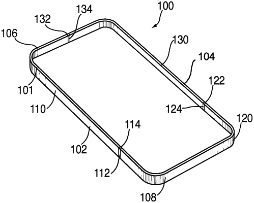
1. An electronic device comprising:
a front cover assembly comprising a front cover defining a front surface of the electronic device;
a back cover assembly comprising a back cover defining a back surface of the electronic device; and
a housing positioned between the front cover assembly and the back cover assembly, the housing comprising:
an outer periphery member positioned between the front cover assembly and the back cover assembly and defining a loop; and
a platform coupled to the outer periphery member and positioned between the front cover assembly and the back cover assembly and defining:
a first mounting surface along a first side of the platform;
a second mounting surface along a second side of the platform; and
an opening extending through the platform;
a first component coupled to the first mounting surface of the platform; and
a second component coupled to the second mounting surface of the platform and operatively coupled to the first component through the opening.