US 12,133,474 B2
Magnetoresistive random access memory and method of manufacturing the same
Hui-Lin Wang, Taipei (TW); Chen-Yi Weng, New Taipei (TW); Chin-Yang Hsieh, Tainan (TW); Yi-Hui Lee, Taipei (TW); Ying-Cheng Liu, Tainan (TW); Yi-An Shih, Changhua County (TW); Jing-Yin Jhang, Tainan (TW); I-Ming Tseng, Kaohsiung (TW); Yu-Ping Wang, Hsinchu (TW); Chien-Ting Lin, Tainan (TW); Kun-Chen Ho, Tainan (TW); Yi-Syun Chou, Taipei (TW); Chang-Min Li, Yunlin County (TW); Yi-Wei Tseng, New Taipei (TW); Yu-Tsung Lai, Tainan (TW); and Jun Xie, Singapore (SG)
Assigned to UNITED MICROELECTRONICS CORP., Hsin-Chu (TW)
Filed by UNITED MICROELECTRONICS CORP., Hsin-Chu (TW)
Filed on Sep. 27, 2023, as Appl. No. 18/373,295.
Application 18/373,295 is a division of application No. 17/835,986, filed on Jun. 9, 2022, granted, now 11,812,669.
Application 17/131,767 is a division of application No. 16/531,129, filed on Aug. 5, 2019, granted, now 10,910,553, issued on Feb. 2, 2021.
Application 17/835,986 is a continuation of application No. 17/131,767, filed on Dec. 23, 2020, granted, now 11,387,408, issued on Jul. 12, 2022.
Claims priority of application No. 201910634906.1 (CN), filed on Jul. 15, 2019.
Prior Publication US 2024/0032439 A1, Jan. 25, 2024
This patent is subject to a terminal disclaimer.
Int. Cl. H10N 50/80 (2023.01); H10B 61/00 (2023.01); H10N 50/01 (2023.01)
CPC H10N 50/80 (2023.02) [H10B 61/00 (2023.02); H10N 50/01 (2023.02)] 5 Claims
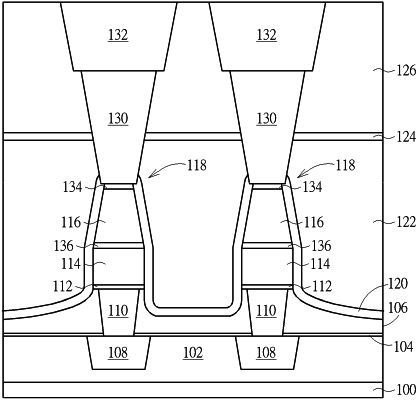
OG exemplary drawing
 
1. A method of fabricating magnetoresistive random access memory, comprising:
providing a substrate;
forming a bottom electrode layer, a magnetic tunnel junction stack, a top electrode layer and a hard mask layer sequentially on said substrate, wherein a material of said top electrode layer is titanium nitride, a material of said hard mask layer is tantalum or tantalum nitride, and a percentage of nitrogen in said titanium nitride gradually decreases from a top surface of top electrode layer to a bottom surface of top electrode layer; and
patterning said bottom electrode layer, said magnetic tunnel junction stack, said top electrode layer and said hard mask layer into multiple magnetoresistive random access memory cells.