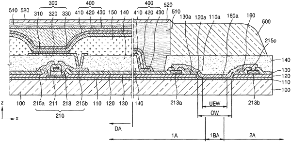
| CPC H10K 77/111 (2023.02) [H10K 50/844 (2023.02); H10K 50/8445 (2023.02); H10K 71/00 (2023.02); H10K 59/1213 (2023.02); H10K 59/40 (2023.02); H10K 2102/311 (2023.02); Y02E 10/549 (2013.01)] | 27 Claims |

|
1. A display device comprising:
a substrate;
a first inorganic insulating layer over the substrate and having a first opening or groove;
a first conductive layer on the first inorganic insulating layer;
a second inorganic insulating layer having contact holes and a second opening or groove on the first conductive layer;
a first organic material layer over the first opening or groove and the second opening or groove, the first organic material layer is continuously disposed within the first opening or groove from directly contacting a first sidewall of the first inorganic insulating layer to directly contacting a second sidewall of the first inorganic insulating layer and is continuously disposed within the second opening or groove from directly contacting a first sidewall of the second inorganic insulating layer to directly contacting a second sidewall of the second inorganic insulating laver;
a second conductive layer on the first organic material layer; and
a second organic material layer on the second conductive layer,
wherein the second conductive layer extends over the first opening or groove and the second opening or groove and electrically contacts to the first conductive layer through the contact holes.
|