| CPC H10K 71/00 (2023.02) [H10K 50/11 (2023.02); H10K 50/81 (2023.02); H10K 50/82 (2023.02); H10K 59/1216 (2023.02); H10K 59/123 (2023.02); H10K 59/124 (2023.02); H10K 59/131 (2023.02); H10K 59/1201 (2023.02); H10K 59/121 (2023.02)] | 11 Claims |

|
1. A display device, comprising:
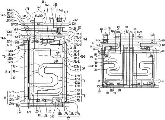
a first pixel and a second pixel which are adjacent to each other in a first direction and symmetrical with respect to a virtual center line extending in a second direction perpendicular to the first direction and disposed between the first pixel and the second pixel;
a first data line and a second data line which are extending in the second direction; and
a first driving voltage line and a second driving voltage line which are extending in the second direction and transmitting a first voltage, wherein
each of the first pixel and the second pixel comprises:
a first transistor including a first node, a second node, and a third node, the first node connected to a gate layer;
a second transistor electrically connected to the second node, the second transistor of the first pixel electrically connected to the first data line, the second transistor of the second pixel electrically connected to the second data line;
a third transistor electrically connected to a scan line and the first node;
a fourth transistor electrically connected to a previous scan line and the first node, the fourth transistor transmitting an initial voltage;
a fifth transistor electrically connected to an emission signal, the second node, and the first voltage;
a sixth transistor electrically connected to the emission signal and an anode of a light emitting element; and
a seventh transistor electrically connected to a control signal and the anode of the light emitting element,
the first transistor comprises the gate layer, and an active layer including a bent portion,
the first data line and the second data line are disposed over the gate layer,
the first data line and the second data line are symmetrical with respect to the virtual center line,
the first driving voltage line and the second driving voltage line are disposed in a same layer as the first data line and the second data line,
the first driving voltage line and the second driving voltage line are symmetrical with respect to the virtual center line,
the first driving voltage line including a first portion extending in the second direction, and a first expansion extruding from the first portion in the first direction,
the second driving voltage line including a second portion extending in the second direction, and second expansion extruding from the second portion in the first direction, and
the first expansion and the second expansion are connected to each other to form one body between the first pixel and the second pixel.
|