| CPC H10K 59/122 (2023.02) [H10K 50/8426 (2023.02); H10K 50/844 (2023.02); H10K 59/124 (2023.02); H10K 71/00 (2023.02); H10K 59/1201 (2023.02)] | 10 Claims |

|
1. A display apparatus comprising:
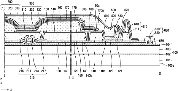
a substrate comprising a display area in which a plurality of thin film transistors and a plurality of display devices electrically connected to the plurality of thin film transistors are arranged over an upper surface of the substrate, and a first non-display area outside the display area;
a through portion penetrating the substrate in a vertical direction;
a second non-display area between the through portion and the display area;
an encapsulation layer on the plurality of display devices and comprising a first inorganic encapsulation layer, an organic encapsulation layer, and a second inorganic encapsulation layer, which are sequentially stacked; and
a planarization layer between the plurality of thin film transistors and the plurality of display devices, the planarization layer extending to a part of the second non-display area and directly contacting another inorganic layer that is under each of the first inorganic encapsulation layer and the planarization layer,
wherein the first inorganic encapsulation layer and the second inorganic encapsulation layer extend to the through portion and directly contact each other in the second non-display area, and the first inorganic encapsulation layer directly contacts the another inorganic layer along an upper surface of the another inorganic layer in the second non-display area, the upper surface of the another inorganic layer being parallel to the upper surface of the substrate,
each of the plurality of display devices comprises a pixel electrode on the planarization layer, an opposite electrode on the pixel electrode, and an intermediate layer between the pixel electrode and the opposite electrode, the another inorganic layer extending between the opposite electrode and the substrate in the display area, and
at least one of the intermediate layer and the opposite electrode extends outside the planarization layer so as to be between the through portion and a portion of the planarization layer that is nearest to the through portion along a lateral direction intersecting the vertical direction.
|