| CPC H10K 59/1213 (2023.02) [H10K 50/844 (2023.02); H10K 59/122 (2023.02)] | 21 Claims |

|
1. A display apparatus comprising:
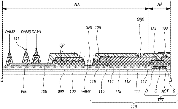
a substrate including a display area in which a plurality of pixels are disposed, and a non-display area surrounding the display area;
a thin film transistor disposed on the substrate;
a first planarization film disposed on the thin film transistor;
a second planarization film disposed under the first planarization film;
a first electrode disposed on the first planarization film and electrically connected to the thin film transistor;
a wiring layer disposed in the non-display area, the wiring layer including multiple outlets; and
a pixel defining layer disposed on the first electrode,
wherein the wiring layer includes:
a common electrode line, and
a common electrode connection line including the multiple outlets,
wherein the non-display area includes:
a dam disposed to surround the display area,
a first groove formed in a first region of the non-display area, the first groove including a first hole extending through both of the pixel defining layer and the first planarization film, and
a second groove formed in a second region of the non-display area, the second groove including a second hole extending through the pixel defining layer, the second region being different from the first region,
wherein a plurality of outlets among the multiple outlets in the wiring layer are located on opposite sides of the first groove,
wherein the first groove and the second groove are located between the dam and the display area, and
wherein the common electrode connection line directly contacts a side surface of the second planarization film, an upper surface of the second planarization film, a side surface of the first planarization film and an upper surface of the first planarization film.
|