| CPC H10K 50/844 (2023.02) [H10K 50/8426 (2023.02); H10K 50/86 (2023.02); H10K 59/12 (2023.02); H10K 59/40 (2023.02); H10K 59/60 (2023.02); H10K 59/65 (2023.02); H10K 71/00 (2023.02); H10K 77/111 (2023.02); H10K 2102/311 (2023.02)] | 17 Claims |

|
1. A display device including an active region and a non-active region, the display device comprising:
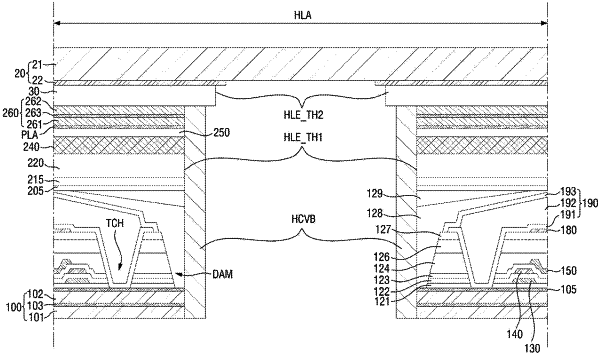
a display panel comprising a plurality of pixels in the active region, the display panel including a first surface, a second surface facing the first surface and a first through hole penetrating from the first surface to the second surface;
a transparent bonding layer on the first surface of the display panel; and
a window layer on the transparent bonding layer, the window layer comprises a base and a print layer defining an optical opening inside on the base,
wherein the optical opening overlaps the first through hole, and
an inner diameter of the optical opening defined in the print layer is smaller than an inner diameter of the first through hole penetrating the display panel.
|