| CPC H10K 50/8426 (2023.02) [H10K 71/00 (2023.02); H10K 50/865 (2023.02); H10K 59/131 (2023.02)] | 5 Claims |
|
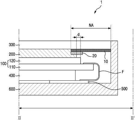
1. A method of manufacturing a display device, the method comprising:
applying a photocurable resin to a display panel using a resin discharge nozzle;
bonding a window including a first pattern and a second pattern to the display panel such that at least a portion of the applied resin is in contact with a lower surface of the second pattern; and
curing the applied resin by irradiating light to the applied resin,
wherein the first pattern and the second pattern, which is arranged in contact with a first portion of a lower surface of the first pattern and has a higher surface free energy than the first pattern, are arranged at a lower surface of the window, and a second portion of the lower surface of the first pattern is exposed.
|