| CPC H10B 43/20 (2023.02) [H10B 43/30 (2023.02); H10B 43/40 (2023.02)] | 20 Claims |

|
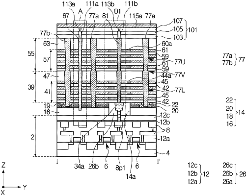
1. A semiconductor device comprising:
a lower structure;
a pattern structure on the lower structure;
a first stack structure and a second stack structure on the lower structure
a separation structure penetrating through the first stack structure;
a memory vertical structure penetrating through the first stack structure and contacting the pattern structure; and
a contact plug penetrating through the second stack structure,
wherein the first stack structure includes first insulating layers and conductive layers alternately stacked in a vertical direction,
wherein the second stack structure includes second insulating layers and third insulating layers alternately stacked in the vertical direction,
wherein the third insulating layers include a material different from a material of the second insulating layers,
wherein the contact plug includes:
a first plug portion penetrating through a plurality of lower insulating layers of the third insulating layers; and
a second plug portion penetrating through a plurality of upper insulating layers of the third insulating layers, and
wherein a lateral surface of the contact plug includes a bent portion between a lateral surface of the first plug portion and a lateral surface of the second plug portion.
|