| CPC H10B 41/27 (2023.02) [H01L 29/66825 (2013.01); H01L 29/66833 (2013.01); H01L 29/788 (2013.01); H01L 29/792 (2013.01); H10B 43/27 (2023.02)] | 9 Claims |

|
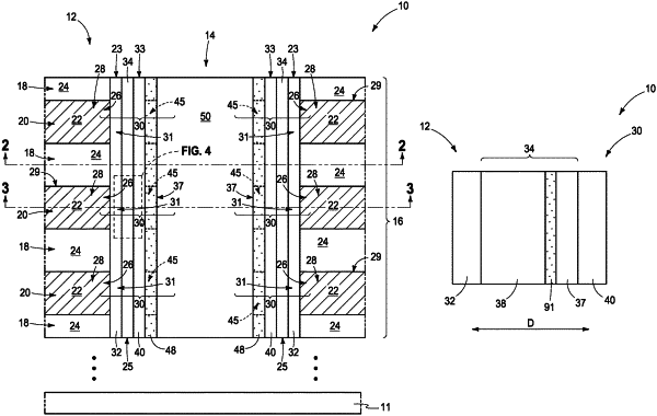
1. A method used in forming a memory cell, comprising:
forming channel material;
forming charge-passage material;
forming programmable material;
forming a charge-blocking region;
forming a control gate; and
the programmable material being formed to comprise at least two regions comprising SiNx having a region comprising SiOy therebetween, where “x” is 0.5 to 3.0 and “y” is 1.0 to 3.0, the forming of the programmable material comprising one of “a” and “b”, where:
(a): forming the SiNx; and
exposing the SiNx to oxygen-containing material to transform some of the SiNx to the SiOy that is directly against remaining of the SiNx; and
(b): forming the SiNx; and
depositing the SiOy against the SiNx by one of chemical vapor deposition, atomic layer deposition, or physical vapor deposition.
|