| CPC H10B 41/27 (2023.02) [G11C 5/06 (2013.01); H01L 23/5384 (2013.01); H01L 23/5386 (2013.01); H01L 29/0649 (2013.01); H10B 43/27 (2023.02)] | 20 Claims |
|
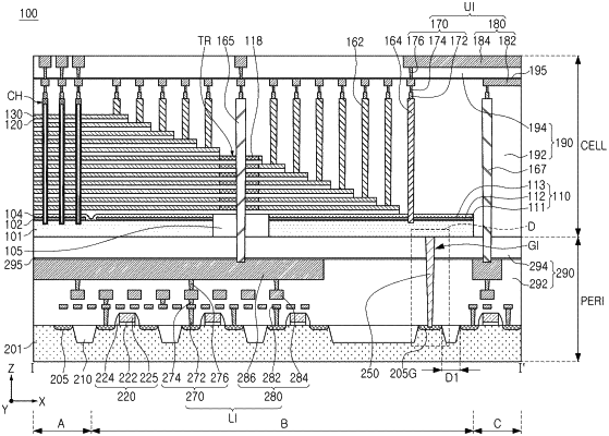
1. A semiconductor device, comprising:
a first semiconductor structure including a first substrate, circuit devices on the first substrate, a lower interconnection structure electrically connected to the circuit devices, and a connection structure,
the first substrate including an impurity region including impurities of a first conductivity type,
the connection structure including a via including a semiconductor of a second conductivity type; and
a second semiconductor structure including a second substrate on the first semiconductor structure, gate electrodes stacked and spaced apart from each other in a first direction perpendicular to an upper surface of the second substrate, and channel structures penetrating the gate electrodes,
the second substrate including a semiconductor of the first conductivity type,
the channel structures extending perpendicular to the second substrate, and
the channel structures each including a channel layer, and
the second semiconductor structure being connected to the impurity region of the first substrate through the connection structure.
|