|
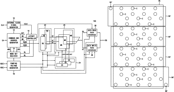
1. A semiconductor memory device comprising: a plurality of memory cell array banks, each comprising a plurality of memory cells provided in a predetermined pattern between a plurality of sub word lines and a plurality of bit lines on a substrate; and a plurality of pumping voltage generators each comprising at least one pumping capacitor provided in a peripheral circuit area on the substrate, wherein each of the plurality of memory cells comprises an access transistor and a first cell capacitor, wherein the at least one pumping capacitor comprises a first sub pumping capacitor group comprising n second cell capacitors and a second sub pumping capacitor group comprising n third cell capacitors, wherein the first sub pumping capacitor group and the second sub pumping capacitor group are connected in series, wherein i second cell capacitors among the n second cell capacitors of the first sub pumping capacitor group are connected in parallel, (n−i) second cell capacitors of the first sub pumping capacitor group are floated, i third cell capacitors among the n third cell capacitors of the second sub pumping capacitor group are connected in parallel, and (n−i) third cell capacitors of the second sub pumping capacitor group are floated, and wherein n and i are positive integers.
|