| CPC H05K 3/3436 (2013.01) [H05K 1/0268 (2013.01); H05K 1/113 (2013.01); H05K 1/186 (2013.01); H05K 3/0017 (2013.01)] | 13 Claims |

|
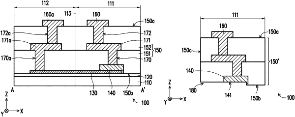
1. A fabrication method of a circuit structure, comprising:
providing a substrate, wherein the substrate includes a main region and a peripheral region;
fabricating a test circuit component on the substrate, wherein the test circuit component comprises one part corresponding to the main region and the other part corresponding to the peripheral region;
fabricating a solder pad on the test circuit component;
fabricating an insulating layer, wherein a second surface of the insulating layer covers the test circuit component and the solder pad, and the insulating layer comprises one part corresponding to the main region and the other part corresponding to the peripheral region;
fabricating a conductive pad on the insulating layer, wherein the conductive pad is coupled to the solder pad;
fabricating a test pad on the insulating layer, wherein the test pad is coupled to the solder pad;
performing a circuit testing step to confirm an electrical coupling condition between the conductive pad and the solder pad;
separating the substrate;
removing the other part of the test circuit component, the other part of the insulating layer and the test pad after the substrate is separated; and
removing the one part of the test circuit component after performing the circuit testing step and removing the other part of the test circuit component, the other part of the insulating layer and the test pad.
|