|
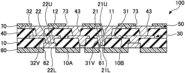
1. A wiring substrate comprising: an insulating layer; a pad in a via hole piercing through the insulating layer, the pad being exposed at a first surface of the insulating layer; a via conductor on the pad in the via hole; and a wiring part on a second surface of the insulating layer facing away from the first surface, the wiring part being connected to the pad through the via conductor in the via hole, wherein a diameter of the pad, a diameter of the via conductor, and a diameter of the via hole are equal to one another at an interface between the pad and the via conductor.
|