| CPC H05K 1/113 (2013.01) [H05K 3/429 (2013.01); H05K 2201/096 (2013.01); H05K 2201/09827 (2013.01); H05K 2203/0554 (2013.01)] | 16 Claims |

|
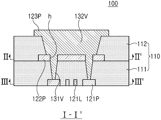
1. A printed circuit board comprising:
an insulating member;
a first pad disposed in the insulating member;
a plurality of first vias respectively disposed on a lower side of the first pad in the insulating member and connected to the first pad;
a second via disposed on an upper side of the first pad in the insulating member and connected to the first pad;
a plurality of second pads disposed on lower sides of the plurality of first vias in the insulating member and connected to the plurality of first vias; and
one or more lines disposed on substantially the same level as the plurality of second pads in the insulating member and disposed between the plurality of second pads,
wherein the first pad has one or more through-holes, and
the plurality of first vias and the second via are integrated as one body through the one or more through-holes.
|