| CPC H05B 45/355 (2020.01) [H02M 1/4233 (2013.01); H02M 3/1582 (2013.01); H05B 45/375 (2020.01); H05B 45/38 (2020.01)] | 9 Claims |
|
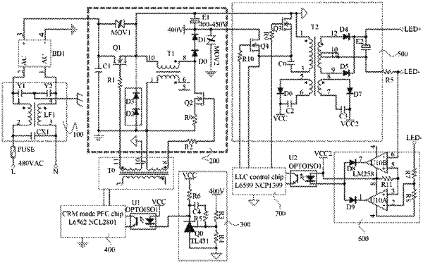
1. A floating type boost-buck power factor correction (PFC) circuit, comprising a filter circuit, a rectifier bridge, a PFC control chip and a voltage sampling circuit, and further comprising a PFC circuit, wherein the PFC circuit comprises a first switching transistor (Q1) and a second switching transistor (Q2) with a withstand voltage of 600 V to 650 V, an energy storage inductor (T1), a freewheel diode (D0), a freewheel diode (D1), an electrolytic capacitor (E1) with a withstand voltage of 400 V to 450 V, a resistor (R0) and a capacitor (C1), wherein
an external alternating current voltage is connected to an input end of the rectifier bridge through the filter circuit; a positive output end of the rectifier bridge is respectively connected with a drain of the first switching transistor (Q1) and one end of the capacitor (C1); a source of the first switching transistor (Q1) is respectively connected with one input end of the energy storage inductor (T1) and one end of the electrolytic capacitor (E1); one end of the electrolytic capacitor (E1) is grounded; one output end in the energy storage inductor (T1) is respectively connected with a positive pole of the freewheel diode (D0) and a drain of the second switching transistor (Q2); a negative pole of the freewheel diode (D0) is connected with the other end of the electrolytic capacitor (E1) through the freewheel diode (D1); the other end of the electrolytic capacitor (E1) is connected with an input end of the voltage sampling circuit; an output end of the voltage sampling circuit is connected with an input end of the PFC control chip through an optically coupled isolator (U1); an output end of the PFC control chip is connected with a primary coil in an isolated drive winding (T0);
a source of the second switching transistor (Q2) is connected with one end of the resistor (R0); a gate of the second switching transistor (Q2) is connected with one end of a first secondary coil in the isolated drive winding (T0) through a resistor (R2); the other end of the first secondary coil in the isolated drive winding (T0) is connected with the other end of the resistor (R0); a gate of the switching transistor (Q1) is connected with one end of a second secondary coil in the isolated drive winding (T0) through a resistor (R1); and the other end of the second secondary coil in the isolated drive winding (T0), the other end of the resistor (R0), the other input end in the energy storage inductor (T1) and the other end of the capacitor (C1) are all grounded.
|