| CPC H04N 25/75 (2023.01) [H04N 25/768 (2023.01); H04N 25/772 (2023.01); H04N 25/778 (2023.01); H04N 25/79 (2023.01)] | 14 Claims |

|
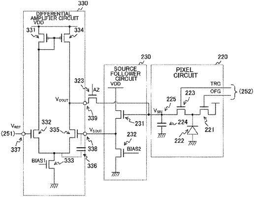
1. A solid-state imaging element comprising:
a differential amplifier circuit that amplifies a difference between potentials of a pair of input nodes and outputs the difference from an output node;
a transfer transistor that transfers charge from a photoelectric conversion element to a floating diffusion layer;
an auto-zero transistor that short-circuits the floating diffusion layer and the output node in a predetermined period; and
a source follower circuit that supplies a potential to one of the pair of input nodes according to a potential of the floating diffusion layer, wherein
the differential amplifier circuit includes:
first and second differential transistors; and
a first current source transistor that is commonly connected to sources of the first and second differential transistors and that supplies a first predetermined current, wherein
a predetermined reference signal is inputted to a gate of the first differential transistor, and
the potential from the source follower circuit is inputted to a gate of the second differential transistor.
|