| CPC H03K 17/6871 (2013.01) [H03F 3/21 (2013.01); H03K 19/17772 (2013.01); H03K 19/20 (2013.01)] | 35 Claims |
|
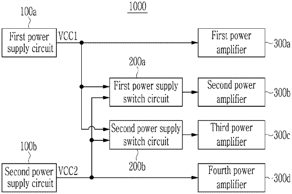
1. A power supply switch circuit, comprising:
a first transistor that switches supplying of a first power supply voltage to a power supply terminal of a power amplifier;
a switch controller that controls the first transistor and to which a second power supply voltage is applied; and
a voltage selector that selects a higher voltage among the first power supply voltage and the second power supply voltage,
wherein the selected higher voltage is applied to a body terminal of the first transistor or a gate terminal of the first transistor.
|