| CPC H03K 17/08122 (2013.01) [H01L 23/62 (2013.01); H01L 29/2003 (2013.01)] | 14 Claims |

|
1. An electronic circuit comprising:
a GaN FET power switch; and
a driver for the GaN FET power switch, the driver including:
a reference device for generating a reference voltage,
a GaN-based under-voltage detector having a first input terminal receiving a supply voltage, a second input terminal for receiving a voltage at ground potential, a third input terminal receiving the reference voltage, and an output terminal, wherein the reference voltage is referred to the supply voltage, and wherein the GaN-based under-voltage detector outputs an under voltage lock-out signal when the supply voltage is below a low-to-high threshold value, and does not output the under voltage lock-out signal when the supply voltage is above the low-to-high threshold value, and
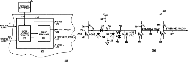
a pulse stretcher having an input terminal coupled to the output terminal of the GaN-based under-voltage detector, and an output terminal for outputting a stretched under voltage lock-out signal for a predetermined amount of time after the supply voltage first rises above the low-to-high threshold value, the pulse stretcher comprising:
a first transistor having a drain, a source coupled to ground potential, and a gate coupled to the input terminal of the pulse stretcher,
a first resistor coupled between the supply voltage and the drain of the first transistor,
a second resistor having one end coupled to the drain of the first transistor,
a first capacitor coupled between another end of the second resistor and ground potential,
a first diode having an anode coupled to the other end of the second resistor, a third resistor having one end coupled to a cathode of the first diode,
a second capacitor coupled between another end of the third resistor and ground potential,
a second diode having an anode coupled to another end of the third resistor,
a third diode having an anode coupled to a cathode of the second diode and a cathode coupled to ground potential,
a second transistor having a drain coupled to the other end of the third resistor, a source coupled to ground potential, and a gate coupled to the input terminal of the pulse stretcher,
a third transistor having a drain, a gate coupled to the other end of the third resistor, and a source coupled to ground potential, and
a fourth resistor coupled between the supply voltage and the drain of the third transistor,
wherein the stretched under voltage lock-out signal is produced at the drain of the third transistor.
|