| CPC H02M 3/33573 (2021.05) [H02M 1/0009 (2021.05); H02M 1/0054 (2021.05); H02M 1/088 (2013.01); H02M 3/01 (2021.05); H02M 3/33576 (2013.01)] | 6 Claims |

|
1. An adaptive load optimization method for a resonant gate drive circuit, wherein:
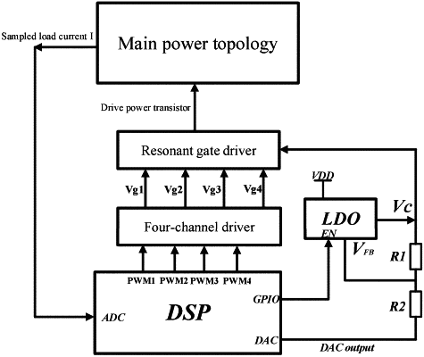
modules adopted by the method comprise a main power topology, a resonant gate driver, a four-channel driver, a low dropout regulator chip, a digital signal processor chip, a first feedback resistor and a second feedback resistor; wherein the main power topology outputs a sampled load current to the digital signal processor chip, the digital signal processor chip outputs six paths of signals, four paths of signals of the six paths of signals include four pulse-width modulation (PWM) channels connected to the four channel driver, the four pulse-width modulation (PWM) channels comprising a first PWM waveform port, a second PWM waveform port, a third PWM waveform port and a fourth PWM waveform port; the four-channel driver correspondingly outputs a plurality of signals to drive the resonant gate driver, the plurality of signals comprising a Q1 gate voltage, a Q2 gate voltage, a Q3 gate voltage and a Q4 gate voltage; a general-purpose input-output port of the digital signal processor chip is connected to an enable pin of the low dropout regulator chip; a digital-to-analog converter terminal of the digital signal processor chip is connected to the resonant gate driver using the first feedback resistor and the second feedback resistor which are connected in series, a midpoint of the first feedback resistor and the second feedback resistor is connected to a full-bridge pin of the low dropout regulator chip, an output voltage port of the low dropout regulator chip is connected to the resonant gate driver, and the resonant gate driver outputs a power switch transistor drive signal to control the main power topology,
wherein multiple power switch transistors of the main power topology are driven by the resonant gate driver, and the resonant gate driver is composed of four metal-oxide-semiconductor field effect transistors (MOSFETs) and an isolation transformer; wherein a first MOSFET and a second MOSFET of the four MOSFETs form a first half-bridge, and a midpoint of the first half-bridge is connected to a dotted terminal of a primary side of the isolation transformer and drives a fourth switch transistor of the main power topology using a midpoint of a bridge arm; and a third MOSFET and a fourth MOSFET of the four MOSFETs form a second half-bridge, and a midpoint of the second half-bridge is connected to a non-dotted terminal of the primary side of the isolation transformer using a port and drives a second switch transistor of the main power topology, and
wherein a coil is arranged on a secondary side of the isolation transformer; wherein in case of two complementary isolation drivers, two coils are arranged on the secondary side, a dotted terminal of the coil at an upper end of the secondary side is connected to one terminal of a first gate parasitic capacitor of a first switch transistor of the main power topology, and a non-dotted terminal of the coil at the upper end of the secondary side is connected to the other terminal of the first gate parasitic capacitor in an ungrounded manner; and a non-dotted terminal of the coil at a lower end of the secondary side is connected to one terminal of a third gate parasitic capacitor of a third switch transistor of the main power topology, and a dotted terminal of the coil at the lower end of the secondary side is connected to the other terminal of the third gate parasitic capacitor in an ungrounded manner.
|