| CPC H02J 7/00304 (2020.01) [H01M 10/4264 (2013.01); H01M 10/44 (2013.01); H02J 7/0031 (2013.01); H03K 3/0231 (2013.01); H03K 17/0822 (2013.01)] | 17 Claims |

|
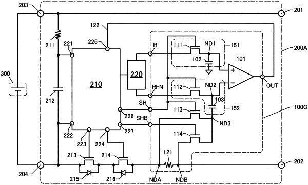
1. A battery pack comprising:
first to fourth transistors and a comparator;
a control circuit electrically connected to gate electrodes of the first to fourth transistors; and
a secondary battery electrically connected to the control circuit,
wherein one of a source and a drain of the first transistor is electrically connected to a non-inverting input terminal of the comparator,
wherein one of a source and a drain of the second transistor is electrically connected to an inverting input terminal of the comparator,
wherein one of a source and a drain of the third transistor is electrically connected to one of a source and a drain of the fourth transistor,
wherein a first resistor is included between the other of the source and the drain of the third transistor and the other of the source and the drain of the fourth transistor,
wherein a first capacitor is electrically connected to the one of the source and the drain of the first transistor,
wherein a second capacitor is included between the one of the source and the drain of the second transistor and the one of the source and the drain of the third transistor, and
wherein each of the first and second transistors comprises an oxide semiconductor in a semiconductor layer.
|