| CPC H01S 5/02423 (2013.01) [H01S 3/0941 (2013.01); H01S 5/02407 (2013.01); C25D 1/02 (2013.01); C25D 5/02 (2013.01); C25D 15/00 (2013.01); H01S 5/4031 (2013.01)] | 10 Claims |
|
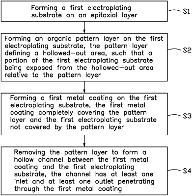
1. A manufacturing method for laser chip, comprising the following steps:
step S1, forming a first electroplating layer on an epitaxial layer;
step S2, forming a pattern layer on the first electroplating layer, the pattern layer having a hollowed-out area, a portion of the first electroplating layer being exposed from the pattern layer through the hollowed-out area;
step S3, forming a first metal coating on the first electroplating layer, the first metal coating completely covering the pattern layer and the first electroplating layer not covered by the pattern layer; and
step S4, removing the pattern layer to form a hollow micropipe between the first metal coating and the first electroplating layer, the hollow micropipe having at least one inlet and at least one outlet penetrating through the first metal coating.
|