| CPC H01L 33/62 (2013.01) [H01L 33/005 (2013.01); H01L 33/22 (2013.01); H01L 33/44 (2013.01); H01L 33/58 (2013.01); H01L 2933/0025 (2013.01); H01L 2933/0058 (2013.01); H01L 2933/0066 (2013.01)] | 14 Claims |

|
1. An optoelectronic component comprising:
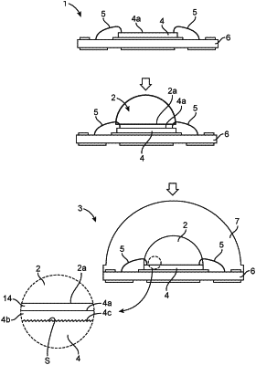
a first joining partner comprising an LED chip with a structured light-emitting surface and a compensation layer applied to the light-emitting surface, wherein the compensation layer has a surface facing away from the light-emitting surface and spaced apart from the light-emitting surface, and wherein the surface forms a first connecting surface;
a second joining partner having a second connecting surface, the first and second connecting surfaces being arranged so that they face each other; and
a bonding layer made of a film of low-melting glass having a layer thickness of not more than 1 μm, wherein the bonding layer bonds the first and second connecting surfaces together,
wherein a structure of the light-emitting surface is encapsulated within the compensation layer such that the structure of the light-emitting surface is vertically displaced from a top surface of the compensation layer,
wherein the first and second connecting surfaces are smooth such that their surface roughness, expressed as center-line roughness, is less than or equal to 50 nm,
wherein the LED chip comprises a semiconductor layer having the light-emitting surface,
wherein a refractive index of the compensation layer is smaller than a refractive index of the semiconductor layer and greater than a refractive index of a material forming the second joining partner.
|