| CPC H01L 33/504 (2013.01) [H01L 27/156 (2013.01); H01L 33/005 (2013.01); H01L 33/486 (2013.01); H01L 33/62 (2013.01); H01L 2933/0041 (2013.01); H01L 2933/0066 (2013.01)] | 12 Claims |
|
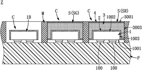
1. A light-emitting diode (LED) package structure, comprising:
an LED chip having two exposed conductive pads;
a quantum dot material layer enclosing the LED chip; and
a blue light scattering material layer disposed on the quantum dot material layer,
wherein a bottom surface of the blue light scattering material layer and a bottom side of the LED chip are flush with each other.
|