| CPC H01L 31/022441 (2013.01) [H01L 31/0682 (2013.01); Y02E 10/547 (2013.01)] | 13 Claims |
|
10. A method of fabricating a photovoltaic assembly, the method comprising:
providing a plurality of substrates, each substrate having a back surface and an opposing light-receiving surface;
forming a plurality of alternating N-type and P-type semiconductor regions in or above the back surface of each of the plurality of substrates, wherein each of the plurality of alternating N-type and P-type semiconductor regions is along a first direction;
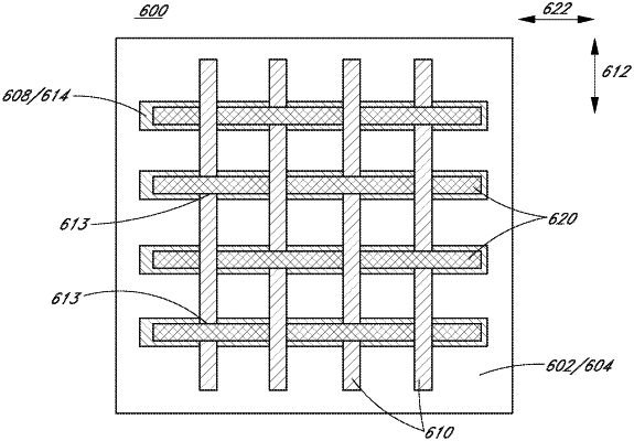
forming a conductive contact structure on the plurality of alternating N-type and P-type semiconductor regions of each of the substrates, the conductive contact structure comprising a plurality of metal wires, wherein each metal wire of the plurality of metal wires is parallel along a second direction to form a one-dimensional layout of a metallization layer for each of the substrates, the second direction orthogonal to the first direction, wherein one or more wires of the plurality of metal wires is common to two or more of the plurality of substrates, and wherein each metal wire of the plurality of metal wires is continuously undulating between and extending beyond two bonding points coupling the metal wire to the plurality of alternating N-type and P-type semiconductor regions; and
forming a plurality of insulating wires, wherein each insulating wire of the plurality of insulating wires is parallel along the first direction, wherein each insulating wire of the plurality of insulating wires is vertically over and parallel with a corresponding one of the plurality of alternating N-type and P-type semiconductor regions, wherein each of the insulating wires is continuous over the corresponding one of the plurality of alternating N-type and P-type semiconductor regions, and wherein each of the insulating wires has a width in the second direction less than a width of the corresponding one of the plurality of alternating N-type and P-type semiconductor regions in the second direction.
|