US 12,132,121 B2
Semiconductor device and manufacturing method thereof
Shunpei Yamazaki, Setagaya (JP); and Satoshi Shinohara, Fujisawa (JP)
Assigned to Semiconductor Energy Laboratory Co., Ltd., Atsugi (JP)
Filed by Semiconductor Energy Laboratory Co., Ltd., Atsugi (JP)
Filed on Feb. 9, 2023, as Appl. No. 18/107,559.
Application 18/107,559 is a continuation of application No. 17/308,658, filed on May 5, 2021, granted, now 11,588,058.
Application 17/308,658 is a continuation of application No. 16/847,912, filed on Apr. 14, 2020, granted, now 11,011,652, issued on May 18, 2021.
Application 16/847,912 is a continuation of application No. 16/053,188, filed on Aug. 2, 2018, granted, now 10,658,522, issued on May 19, 2020.
Application 16/053,188 is a continuation of application No. 15/645,217, filed on Jul. 10, 2017, granted, now 10,043,918, issued on Aug. 7, 2018.
Application 15/645,217 is a continuation of application No. 15/356,976, filed on Nov. 21, 2016, abandoned.
Application 15/356,976 is a continuation of application No. 14/933,392, filed on Nov. 5, 2015, granted, now 9,530,897, issued on Dec. 27, 2016.
Application 14/933,392 is a continuation of application No. 14/590,133, filed on Jan. 6, 2015, granted, now 9,196,745, issued on Nov. 24, 2015.
Application 14/590,133 is a continuation of application No. 13/527,882, filed on Jun. 20, 2012, granted, now 8,952,377, issued on Feb. 10, 2015.
Claims priority of application No. 2011-152099 (JP), filed on Jul. 8, 2011.
Prior Publication US 2023/0275159 A1, Aug. 31, 2023
Int. Cl. H01L 29/786 (2006.01); H01L 29/04 (2006.01); H01L 29/24 (2006.01)
CPC H01L 29/78696 (2013.01) [H01L 29/045 (2013.01); H01L 29/24 (2013.01); H01L 29/786 (2013.01); H01L 29/7869 (2013.01); H01L 29/78693 (2013.01)] 15 Claims
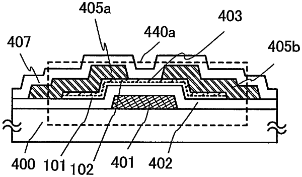
OG exemplary drawing
 
1. A semiconductor device comprising:
a gate electrode;
a gate insulating film over the gate electrode;
a first oxide semiconductor layer over the gate insulating film;
a second oxide semiconductor layer over and in contact with the first oxide semiconductor layer;
a first conductive layer over and in electrical contact with the second oxide semiconductor layer;
a second conductive layer over and in electrical contact with the second oxide semiconductor layer; and
an oxide insulating layer over the first conductive layer, the second conductive layer, and the second oxide semiconductor layer,
wherein the first oxide semiconductor layer comprises indium, tin, and zinc,
wherein the second oxide semiconductor layer comprises indium, gallium, and zinc,
wherein an atomic ratio of indium to tin in the first oxide semiconductor layer is greater than an atomic ratio of indium to gallium in the second oxide semiconductor layer, and
wherein a c-axis of a crystal in the second oxide semiconductor layer is perpendicular to an upper surface of the second oxide semiconductor layer.