| CPC H01L 29/78391 (2014.09) [H01L 22/12 (2013.01); H01L 29/516 (2013.01); H01L 29/6684 (2013.01); H01L 29/0665 (2013.01); H01L 29/42392 (2013.01); H01L 29/7851 (2013.01); H01L 29/78696 (2013.01)] | 17 Claims |

|
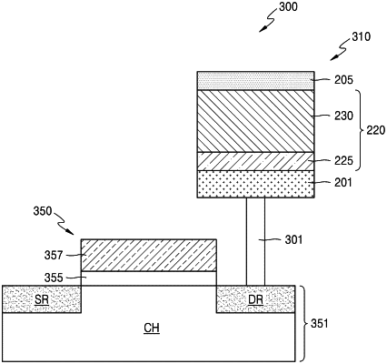
1. A ferroelectric electronic device comprising:
a first layer;
an insulating layer including a first interface and a ferroelectric layer, the first interface adjacent to the first layer, the insulating layer further including a paraelectric layer corresponding to the first interface with the first layer, the paraelectric layer between the first layer and the ferroelectric layer; and
an upper electrode over the insulating layer,
wherein the insulating layer has a bulk defect density per volume of 1016 cm−3eV−1 or more and an interface defect density per area of 1010 cm−2eV−1 or more, and
wherein the paraelectric layer includes at least one of SiO, AlO, SiON, SiN, a native oxide of Ge, or a native oxide of Si.
|