| CPC H01L 29/7835 (2013.01) [H01L 29/401 (2013.01); H01L 29/402 (2013.01); H01L 29/4916 (2013.01); H01L 29/4966 (2013.01); H01L 29/4991 (2013.01); H01L 29/66484 (2013.01); H01L 29/66545 (2013.01); H01L 29/66553 (2013.01); H01L 29/66659 (2013.01); H01L 29/7831 (2013.01)] | 20 Claims |
|
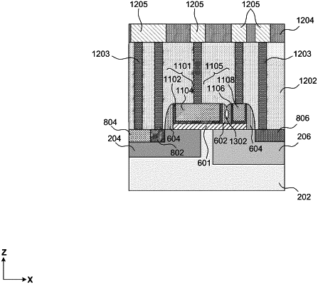
1. A semiconductor structure, comprising:
a substrate;
a channel region disposed in the substrate;
a source region adjacent to the channel region;
a drain region disposed in the substrate;
a drift region adjacent to the drain region;
a dual gate structure, comprising:
a continuous gate dielectric layer disposed directly on the channel region and the drift region;
a first gate stack disposed on the gate dielectric and overlapping with the channel region and the drift region; and
a second gate stack disposed on the gate dielectric, non-overlapping with the channel region, and overlapping with the drift region;
an inner spacer disposed between the first and second gate stacks and in physical contact with the continuous gate dielectric layer:
a first outer spacer disposed along a sidewall of the first gate stack and in physical contact with the channel region; and
a second outer spacer disposed along a sidewall of the second gate stack and in physical contact with the drift region.
|