| CPC H01L 29/7827 (2013.01) [H01L 21/823814 (2013.01); H01L 21/823885 (2013.01); H01L 27/092 (2013.01); H01L 29/0847 (2013.01); H01L 29/42368 (2013.01); H01L 29/66666 (2013.01)] | 20 Claims |

|
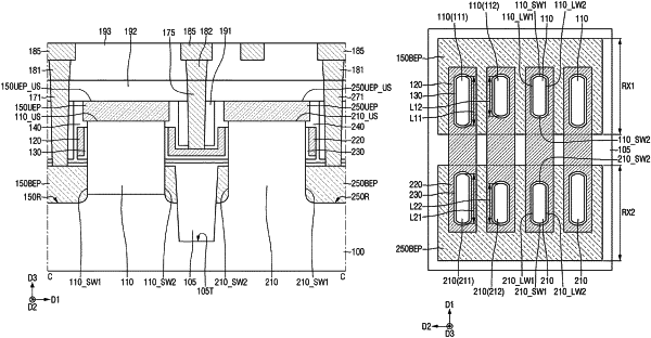
1. A semiconductor device comprising:
an active pattern protruding from a substrate, the active pattern including a first long sidewall and a second long sidewall, the first long sidewall and the second long sidewall extending in a first direction and opposite to each other in a second direction;
a lower epitaxial pattern on the substrate and covering a part of the active pattern;
a gate electrode on the lower epitaxial pattern and extending along the first and second long sidewalls of the active pattern; and
an upper epitaxial pattern on the active pattern and connected to an upper surface of the active pattern,
wherein the active pattern includes short sidewalls connecting with the first and second long sidewalls of the active pattern,
at least one of the short sidewalls of the active pattern has a curved surface, and
a length of the first long sidewall is greater than a length of the second long sidewall.
|