| CPC H01L 29/4238 (2013.01) [H01L 21/76804 (2013.01); H01L 21/823418 (2013.01); H01L 29/0665 (2013.01); H01L 29/4933 (2013.01); H01L 29/6656 (2013.01)] | 19 Claims |

|
1. A method comprising:
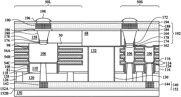
forming a first transistor structure on a semiconductor substrate and a second transistor structure on the semiconductor substrate adjacent the first transistor structure; and
forming a first interconnect structure on a backside of the first transistor structure and the second transistor structure, wherein forming the first interconnect structure comprises:
forming a first contact electrically coupled to a first source/drain region of the first transistor structure; and
forming a second contact electrically coupled to a second source/drain region of the second transistor structure, the second contact having a second length less than a first length of the first contact, wherein a first surface of the first contact opposite the first source/drain region is coplanar with a second surface of the second contact opposite the second source/drain region.
|