| CPC H01L 29/1608 (2013.01) [H01L 21/67288 (2013.01); H01L 22/12 (2013.01)] | 30 Claims |

|
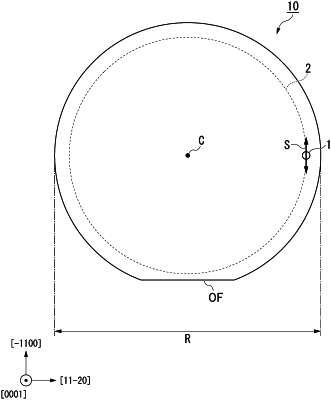
1. A SiC substrate having a warpage factor F of 300 μm or less represented by the following formula (1) obtained from a thickness, a diameter, and a stress at a first outer circumferential end 10 mm inward from an outer circumferential end in the [11-20] direction from a center thereof,
F=K×exp(a+b×ln(σ)+c×ln(R)+d×ln(ts)) (1)
where K, a, b, c, and d are constants satisfying K=1.3373, a=−11.67123, b=1.4030953, c=1.8050972, and d=−1.585898,
σ satisfies σ=60 (MPa)−⅔×S (MPa),
S is internal stress in the <1-100> direction, which is the same direction as a circumferential direction of the first outer circumferential end, and in which tensile stress is defined as positive and compressive stress is defined as negative,
ts is the thickness (mm),
R is the diameter (mm), and
Wherein the diameter is 290 mm or more.
|