| CPC H01L 27/156 (2013.01) [H01L 33/08 (2013.01); H01L 33/382 (2013.01); H01L 33/62 (2013.01); H10K 59/1213 (2023.02); H10K 59/122 (2023.02); H10K 59/123 (2023.02); H01L 33/38 (2013.01); H10K 59/124 (2023.02)] | 22 Claims |

|
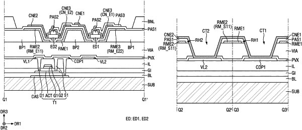
1. A display device comprising:
conductive layers on a substrate;
a via layer on the conductive layers;
a first electrode and a second electrode extending in one direction on the via layer and spaced from each other;
a first insulating layer on the first electrode and the second electrode;
a plurality of light emitting elements on the first insulating layer, each of the light emitting elements having one end on the first electrode and an other end on the second electrode; and
a first connection electrode and a second connection electrode on the first insulating layer, the first connection electrode overlapping the first electrode, and the second connection electrode overlapping the second electrode,
wherein the first connection electrode and the second connection electrode are in contact with the conductive layers through contact portions.
|