| CPC H01L 27/14685 (2013.01) [H01L 27/14603 (2013.01); H01L 27/14612 (2013.01)] | 15 Claims |
|
1. An image sensing device comprising:
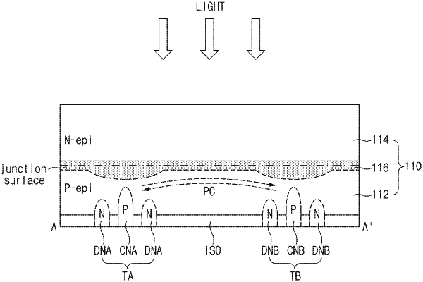
a first substrate layer including first conductive impurities and structured to produce photocharges based on incident light and capture the photocharges using a voltage difference induced in response to a demodulation control signal;
a second substrate layer including second conductive impurities having characteristics opposite to those of the first conductive impurities, and structured to be bonded to the first substrate layer; and
a depletion layer formed between the first substrate layer and the second substrate layer,
wherein the first substrate layer includes a plurality of first substrate layer taps, and
wherein the plurality of first substrate layer taps includes:
a first control node and a second control node spaced apart from each other by a predetermined distance and configured to generate a pixel current in the first substrate layer based on the demodulation control signal;
a first detection node formed to surround the first control node; and
a second detection node formed to surround the second control node.
|