| CPC H01L 27/14636 (2013.01) [H01L 27/14625 (2013.01); H01L 27/14634 (2013.01); H04N 23/55 (2023.01)] | 18 Claims |

|
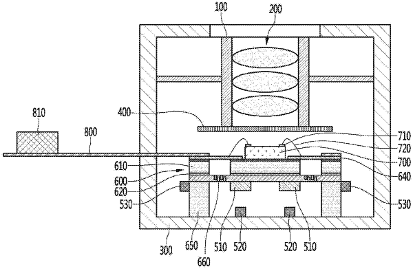
1. An image sensor substrate comprising:
a spring plate;
an insulating layer disposed on the spring plate; and
a conductive pattern part disposed on the insulating layer,
wherein the insulating layer includes:
a first insulating part;
a second insulating part disposed surrounding a periphery of the first insulating part and spaced apart from the first insulating part with a first open region interposed therebetween; and
an extension insulating part disposed in the first open region and connecting between the first insulating part and the second insulating part,
wherein the conductive pattern part includes:
a first conductive pattern part disposed on the first insulating part;
a second conductive pattern part disposed on the second insulating part; and
an extension pattern part disposed on the extension insulating part and interconnecting the first and second conductive pattern parts,
wherein the spring plate includes an elastic member disposed under the extension insulating part, and
wherein the extension insulating part includes:
an overlapping region overlapping with the elastic member in a thickness direction of the elastic member; and
a non-overlapping region that does not overlap with the elastic member in the thickness direction.
|