| CPC H01L 27/14627 (2013.01) [G02B 5/003 (2013.01); G02B 7/02 (2013.01); H01L 27/14618 (2013.01); H01L 27/1462 (2013.01); H01L 27/14623 (2013.01); H01L 27/14629 (2013.01); H01L 27/14685 (2013.01); G02B 1/113 (2013.01)] | 20 Claims |

|
1. A camera package, comprising:
a solid-state imaging element;
a transparent substrate that protects the solid-state imaging element, wherein the transparent substrate includes:
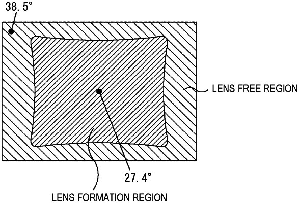
a lens formation region; and
a lens free region around the lens formation region;
a lens on the transparent substrate, wherein the lens is in the lens formation region; and
a plurality of micro-irregularities in the lens free region, wherein a contact angle of the lens free region is different from a contact angle of the lens formation region.
|