| CPC H01L 27/14618 (2013.01) [H01L 27/14683 (2013.01); H01L 31/024 (2013.01)] | 16 Claims |

|
1. A semiconductor device, comprising:
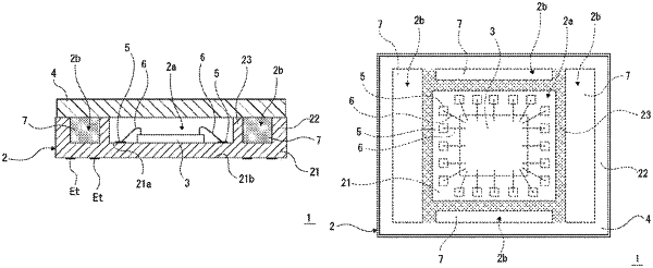
a substrate portion in which an external connection terminal is on a rear surface of the substrate portion, wherein the rear surface is opposite to a front surface of the substrate portion;
a semiconductor chip that mounts on the substrate portion;
an outer wall portion that protrudes toward a side of the front surface in an outer circumferential portion of the substrate portion;
a lid portion which covers the semiconductor chip, wherein the outer wall portion supports the lid portion; and
a heat storage member which at a position further inside than the outer wall portion-between the rear surface of the substrate portion and a rear surface of the lid portion,
wherein the heat storage member fills a space that the lid portion seals,
an electronic component different from the semiconductor chip is included in the space, and
the heat storage member covers the electronic component in the space.
|