| CPC H01L 27/14614 (2013.01) [H01L 27/14616 (2013.01); H01L 27/14636 (2013.01); H04N 25/00 (2023.01); H04N 25/77 (2023.01); H04N 25/78 (2023.01); H04N 23/63 (2023.01)] | 16 Claims |

|
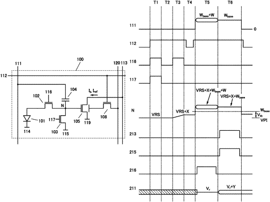
1. An imaging device comprising a pixel, a first circuit, and a second circuit,
wherein the first circuit is configured to supply one of a first potential and a second potential to the pixel,
wherein the second potential is a potential obtained by adding a weight to the first potential,
wherein the pixel is configured to generate first data,
wherein, when the first potential is supplied from the first circuit to the pixel, the pixel is configured to output second data to the second circuit on the basis of the first data and the first potential,
wherein when the second potential is supplied from the first circuit to the pixel, the pixel is configured to output third data to the second circuit on the basis of the first data and the second potential, and
wherein the second circuit is configured to generate fourth data corresponding to a difference between the second data and the third data.
|