| CPC H01L 27/1225 (2013.01) [G02F 1/1368 (2013.01); H01L 27/127 (2013.01)] | 20 Claims |

|
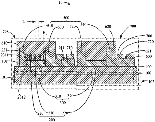
1. A display device, comprising:
a substrate layer, including a first substrate area and a second substrate area adjacent to the first substrate area;
a gate layer disposed on the substrate layer, wherein the gate layer includes a first gate portion and a second gate portion, the first gate portion is located on the first substrate area, and the second gate portion is located on the second substrate area; and
an active layer including a first body portion, a second body portion, and an additional portion, wherein the first body portion is disposed in the first substrate area and on the first gate portion, the additional portion is disposed on the first body portion, the second body portion is disposed in the second substrate area and on the second gate portion, the first body portion and the additional portion are not connected with the second body portion, and a band gap of the additional portion is smaller than a band gap of the first body portion and a band gap of the second body portion,
wherein the additional portion includes a plurality of first additional sub-portions, and each adjacent two of the first additional sub-portions are not connected with each other.
|