| CPC H01L 27/0886 (2013.01) [H01L 21/823821 (2013.01); H01L 23/49827 (2013.01); H01L 27/0924 (2013.01); H01L 29/41791 (2013.01); H01L 29/66795 (2013.01); H01L 29/785 (2013.01)] | 20 Claims |

|
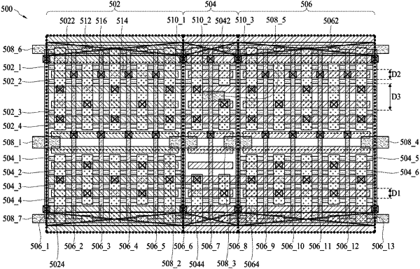
1. An integrated circuit device, comprising:
a first fin structure, having a first type dopant, disposed on a substrate and aligned in a first direction;
a second fin structure, having the first type dopant, disposed on the substrate and aligned in the first direction, wherein the second fin structure is successively adjacent to the first fin structure;
a third fin structure, having a second type dopant, disposed on the substrate in the first direction;
a fourth fin structure, having the second type dopant, disposed on the substrate and aligned in the first direction, wherein the fourth fin structure is successively adjacent to the third fin structure;
a first conductive line, aligned in a second direction, arranged to wrap a first portion of the first fin structure;
a second conductive line, aligned with the first conductive line in the second direction, arranged to wrap a second portion, a third portion, and a fourth portion of the second fin structure, the third fin structure, and the fourth fin structure respectively, wherein the second conductive line is physically disconnected from the first conductive line in the second direction; and
a first conductive via, disposed on the first conductive line, wherein when the second fin structure is activated, the first conductive via is electrically coupled to a reference voltage to disable the first fin structure;
wherein a first distance between the first fin structure and the second fin structure is different from a second distance between the third fin structure and the fourth fin structure.
|