| CPC H01L 27/088 (2013.01) [H01L 29/41775 (2013.01); H01L 29/42372 (2013.01)] | 15 Claims |

|
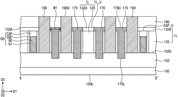
1. A semiconductor device, comprising:
a plurality of gate structures on a substrate, the plurality of gate structures spaced apart from each other in a first direction and extending in a second direction intersecting the first direction;
a plurality of separation patterns penetrating immediately neighboring gate structures of the plurality of gate structures, respectively; and
a lower dielectric layer being between the plurality of gate structures and extending between the plurality of separation patterns,
wherein each of the plurality of separation patterns separates a corresponding one of the neighboring gate structures into a pair of gate structures that are spaced apart from each other in the second direction, and
wherein the plurality of separation patterns are spaced apart from and aligned with each other along the first direction,
wherein each of the plurality of gate structures includes:
a gate electrode extending in the second direction; and
a gate capping pattern on a top surface of the gate electrode,
wherein each of the plurality of separation patterns penetrates the gate capping pattern and the gate electrode that are included in a corresponding one of the neighboring gate structures,
wherein a height of an uppermost surface of each of the plurality of separation patterns is higher than a height of a top surface of the gate capping pattern, and
wherein a height of an uppermost surface of the lower dielectric layer between the plurality of separation patterns is higher than the height of a top surface of the gate capping pattern.
|