| CPC H01L 27/0688 (2013.01) [H01L 21/76898 (2013.01); H01L 21/8221 (2013.01); H01L 23/5283 (2013.01); H01L 27/088 (2013.01); H01L 27/14636 (2013.01); H01L 29/4175 (2013.01); H01L 29/78391 (2014.09); H01L 29/7843 (2013.01); H01L 2225/06541 (2013.01)] | 15 Claims |

|
1. A semiconductor device, comprising:
a lower semiconductor substrate;
an upper semiconductor substrate overlapping the lower semiconductor substrate, the upper semiconductor substrate including a first surface and a second surface opposite to the first surface;
a first upper gate structure on the first surface of the upper semiconductor substrate;
a second upper gate structure on the first surface of the upper semiconductor substrate;
a first interlayer insulation film which covers the first upper gate structure, wherein the first interlayer insulation film is between the lower semiconductor substrate and the upper semiconductor substrate; and
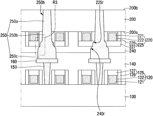
an upper contact connected to the lower semiconductor substrate, wherein the upper contact includes a first protrusion with a curved shape and in contact with a first spacer that extends from the first surface of the upper semiconductor substrate to the first protrusion to form a curved side surface of the first upper gate structure and a second protrusion with a curved shape and in contact with a second spacer that extends from the first surface of the upper semiconductor substrate to the second protrusion to form a curved side surface of the second upper gate structure such that the upper contact is sandwiched between the first and second upper gate structures,
wherein the upper contact includes a first portion penetrating the upper semiconductor substrate, and a second portion having a side surface adjacent to the curved side surface of the first upper gate structure, and
a width of the first portion decreases toward the second surface,
wherein the second portion of the upper contact includes a third protrusion which is adjacent to a bottom surface of the first upper gate structure and protrudes toward the first upper gate structure, the third protrusion being formed on the same side of the upper contact as the first protrusion, the third protrusion being provided in a concave recess overlapped by the first upper gate structure in a direction perpendicular to the first surface of the upper semiconductor substrate, and
wherein the first portion of the upper contact having the decreasing width and the third protrusion sandwich the first protrusion.
|