| CPC H01L 25/167 (2013.01) [H01L 33/44 (2013.01); H01L 33/62 (2013.01); H01L 33/32 (2013.01); H01L 33/36 (2013.01)] | 20 Claims |

|
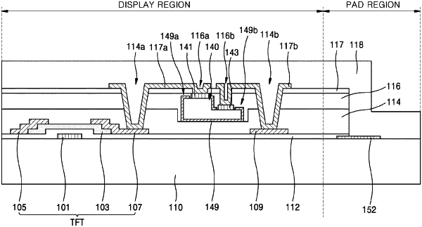
1. A micro light emitting diode (LED) display device, comprising:
a substrate;
a plurality of thin film transistors on the substrate;
a plurality of micro light emitting diodes (LEDs) on the substrate, each of the plurality of micro LEDs including:
a protective film;
an electrode; and
a first contact hole provided in the protective film, wherein the first contact hole exposes a portion of an upper surface of a corresponding micro LED, and wherein the electrode is disposed in the contact hole on the upper surface; and
at least one insulating layer covering the micro LEDs, the at least one insulating layer having a second contact hole to expose an upper surface of the electrode of the corresponding micro LED;
wherein the first contact hole is larger than the second contact hole from a plan view,
wherein a lower surface of the micro LED faces a direction in which the thin film transistors are disposed, and the upper surface of the micro LED faces a direction in which the thin film transistors are not disposed,
wherein the protective film contacts and extends over the upper surface of the electrode, and
wherein the at least one insulating layer contacts a portion of the upper surface of the electrode and fully covers the protective film.
|