| CPC H01L 25/167 (2013.01) [H01L 24/19 (2013.01); H01L 24/24 (2013.01); H01L 24/73 (2013.01); H01L 24/82 (2013.01); H01L 24/96 (2013.01); H01L 33/54 (2013.01); H01L 33/62 (2013.01); H01L 2224/211 (2013.01); H01L 2224/24147 (2013.01); H01L 2224/73209 (2013.01); H01L 2224/82005 (2013.01); H01L 2933/005 (2013.01); H01L 2933/0066 (2013.01)] | 5 Claims |

|
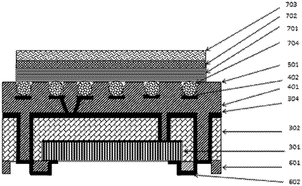
1. A method of packaging a fan-out LED device, comprising steps of:
1) providing a support substrate;
2) forming a separation layer on the support substrate;
3) providing an LED wafer comprising a first surface and a second surface, wherein the first surface is plated with LED electrodes, and the second surface is attached to the separation layer such that the LED electrodes on the first surface of the LED wafer face away from the separation layer;
4) packaging the LED wafer with a packaging layer such that the first surface and a periphery of the LED wafer are enclosed by the packaging layer, wherein the packaging layer at the periphery of the LED wafer is in contact with the separation layer;
5) drilling holes in the packaging layer, wherein the holes expose portions of the first surface of the LED wafer and a surface of the separation layer;
6) plating LED electrodes in the holes such that a surface of the packaging layer, the exposed portions of the first surface of the LED wafer, and the exposed surface of the separation layer are covered by a continuous metal material;
7) forming a first redistribution layer on the packaging layer on the first surface of the LED wafer, wherein the first redistribution layer comprises a first PI dielectric layer and first metal wires, wherein the first PI dielectric layer and the first metal wires are stacked alternately, wherein the first PI dielectric layer also fills the holes at drilled locations of the packaging layer, wherein the first metal wires are connected to the LED electrodes exposed from the packaging layer;
8) peeling the support substrate off the packaged LED wafer, along with the separation layer, to expose the packaging layer, the LED electrodes at the drilled locations of the packaging layer, and the second surface of the LED wafer;
9) forming a second redistribution layer on the second surface of the LED wafer, wherein the second redistribution layer comprises a second PI dielectric layer and second metal wires disposed in the second PI dielectric layer, wherein the second metal wires of the second redistribution layer are connected to the first metal wires of the first redistribution layer to lead out the LED wafer and the LED electrodes; and
10) surface mounting an IC control module with a heat sink to the first redistribution layer.
|