| CPC H01L 25/0753 (2013.01) | 17 Claims |

|
1. A light emitting diode (LED) display panel, comprising a substrate and a plurality of LED devices disposed on the substrate, the plurality of LED devices are arranged in an array, and the substrate is formed by splicing at least two sub-substrates, wherein:
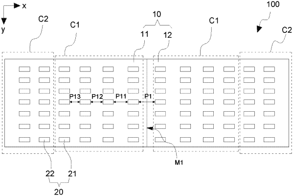
two adjacent ones of the sub-substrates are spliced to form a first splicing seam in a first direction, the first direction intersects an extension direction of the first splicing seam, two adjacent ones of the LED devices located on both ends of the first splicing seam have a first splicing distance therebetween, and the first splicing distance is defined as D1+ΔA1, wherein D1 is a first target pitch, ΔA1 is a first splicing tolerance, and the first splicing tolerance ΔA1 comprises a splicing mechanism tolerance and a sub-substrate size tolerance;
the plurality of LED devices comprise a plurality of first LED devices, a first region is disposed on the sub-substrates located on both sides of the first splicing seam, the first region is located on the sub-substrates close a side of the first splicing seam, and the first region is disposed with the plurality of first LED devices thereon;
a pitch between at least portions of two adjacent ones of the first LED devices gradually decreases from an end close to the first splicing seam to an end away from the first splicing seam in the first region in the first direction, and a pitch between any two adjacent ones of the first LED devices is less than the first splicing distance and greater than the first target pitch;
a pitch between two adjacent ones of the first LED devices gradually decreases from the end close to the first splicing seam to the end away from the first splicing seam in the first region in the first direction, and the D1 is less than or equal to three microns; and
a difference between every two adjacent pitches is same, gradually increases, or gradually decreases in the first region in the first direction from the end close to the first splicing seam to the end away from the first splicing seam.
|